Difference between revisions of "MCE Timing Diagram"
From MCEWiki
| Line 46: | Line 46: | ||
** Due to a firmware bug (revisions prior to 5.1.4), the coadd window is always being adjusted for an ADC latency of 4 (even for Rev. E cards). This throws off the sampling window by 7 cycles in Rev. E cards. (First recorded sample is from clock cycle: sample_dly-7, i.e. one has to make that correction when plugging in a number for sample_dly.) | ** Due to a firmware bug (revisions prior to 5.1.4), the coadd window is always being adjusted for an ADC latency of 4 (even for Rev. E cards). This throws off the sampling window by 7 cycles in Rev. E cards. (First recorded sample is from clock cycle: sample_dly-7, i.e. one has to make that correction when plugging in a number for sample_dly.) | ||
| − | * see [ | + | * see [[Raw-mode readout#Interpretation_of_raw_mode_data]] |
* Bias Card DACs (MAX5443) latch on low-to-high transition of CS (chip-select). Address Card DACs are clocked on the negative edge of the main clock. | * Bias Card DACs (MAX5443) latch on low-to-high transition of CS (chip-select). Address Card DACs are clocked on the negative edge of the main clock. | ||
Revision as of 17:34, 15 November 2011
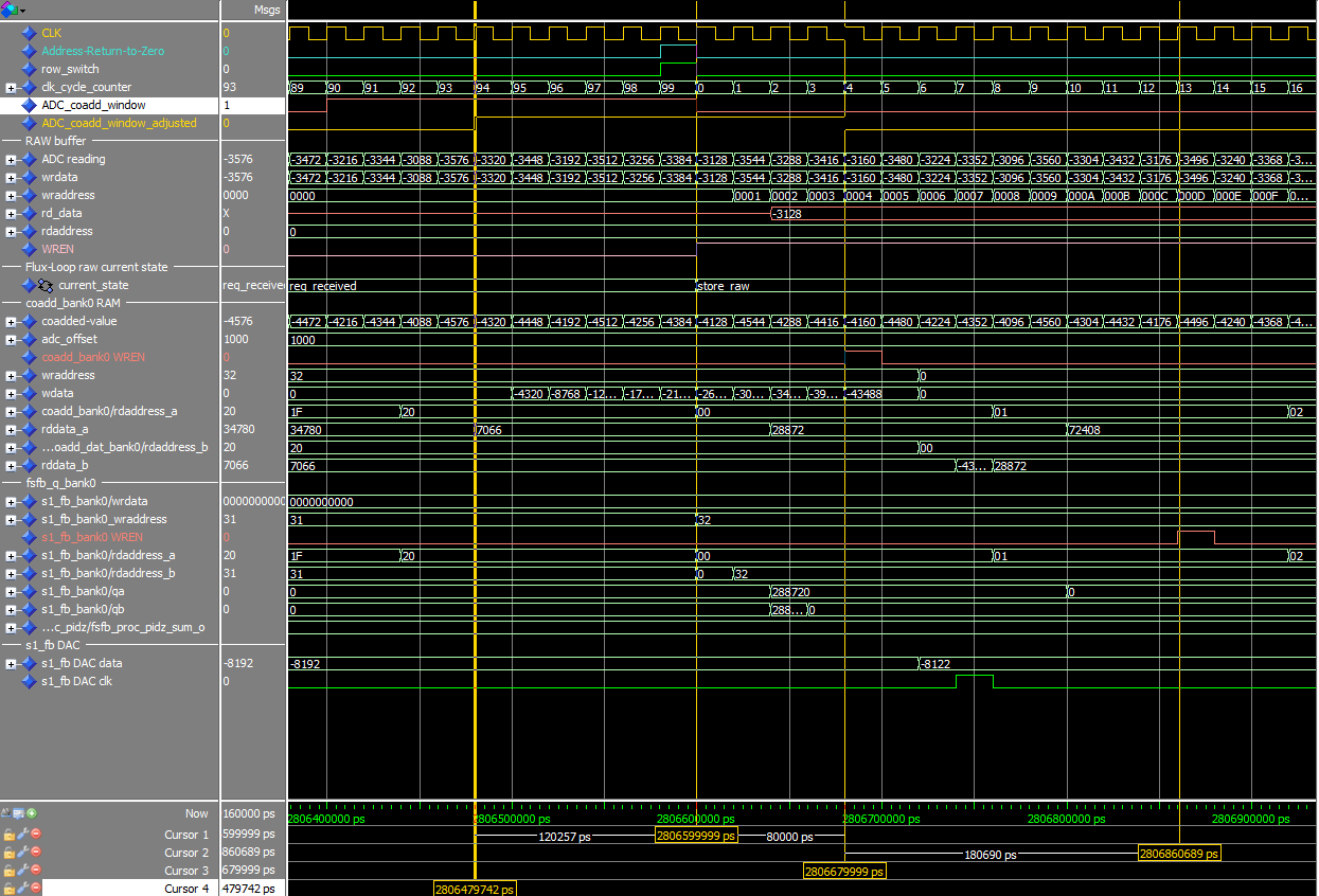
The following timing diagram is generated by simulating MCE firmware using ModelsimTM, therefore, it does not include the analog circuit delays (DAC delay, RC filters, settling time, etc) into account.
 Parameters used for this simulation:
| row_len | 100 |
| num_rows | 33 |
| sample_dly | 40 |
| sample_num | 10 |
| servo_mode | 3 |
| Address Card enbl_mux | 1 |
| Bias Card enbl_mux | 1 |
| RC firmware rev. | 5.1.2 |
| BC firmware rev. | 5.0.5 |
| AC firmware rev. | 5.0.3 |
| CC firmware rev. | 5.0.7 |
Notes
- The coadd window is adjusted to account for the ADC latency. The ADC latency is 4 clock cycles for Rev. B cards and 11 clk cycles for Rev. E cards. When the coadd window is asserted at clock cycle 40 in the diagram above, the samples are stored starting at clock cycle 44 for a Rev. B card.
- Due to a firmware bug (revisions prior to 5.1.4), the coadd window is always being adjusted for an ADC latency of 4 (even for Rev. E cards). This throws off the sampling window by 7 cycles in Rev. E cards. (First recorded sample is from clock cycle: sample_dly-7, i.e. one has to make that correction when plugging in a number for sample_dly.)
- see Raw-mode readout#Interpretation_of_raw_mode_data
- Bias Card DACs (MAX5443) latch on low-to-high transition of CS (chip-select). Address Card DACs are clocked on the negative edge of the main clock.
- In Address Card section, both DAC_clk(0) and DAC_clk(32) are shown. This indicates that first, the previous row's DAC (32 in this case) is turned off and then the new DAC (0 in this case) is turned on. All Address-Card DACs are off for 2 clock cycles.
- Bias Card DACs (MAX5443) have ~400ns settling delay (see FULL-SCALE STEP RESPONSE on page 6 here,
- Address Card and Readout Card DACs (AD9744) have a settling delay of 11 ns, see Table 2, pg 4 ohere
