Readout Card Preamp Chain
The readout card preamp chain consists of four stages of amplification which provide gain and act as a low pass filter. Six RC poles are included in the chain and act together to give a steep roll off which limits out of band noise. The exact pole locations and filter cut off frequency depends upon the particular read out card revision, but the basic topology is consistent across all revisions up to the latest revision (D). This topology consists of two initial low noise amplifier stages each with a single RC pole in their respective feedback loops (R12&C74 followed by R14&C75 in Rev B), followed by a third stage of gain which also includes another RC pole in its feedback loop (R16&C76 in Rev B), and finally a differential ADC driver which has symmetric RC poles on both the positive and negative outputs (R10&C73 and R24&C77 in Rev B). There is also a low pass RC filter between the first and second stages (R20&C78 in Rev B) and third and fourth stages (R21&C79 in Rev B).
The test results shown were produced by collecting raw data sampled at 50 MHz, with the cold electronics replaced by test boards which short all of the instrument backplane lines with 50 ohm resistors. A summary of the results is in the table below.
Readout Card Revision Summary
| Board Revision | Noise (RMS) | Bandwidth | Attenuation at 500 kHz |
|---|---|---|---|
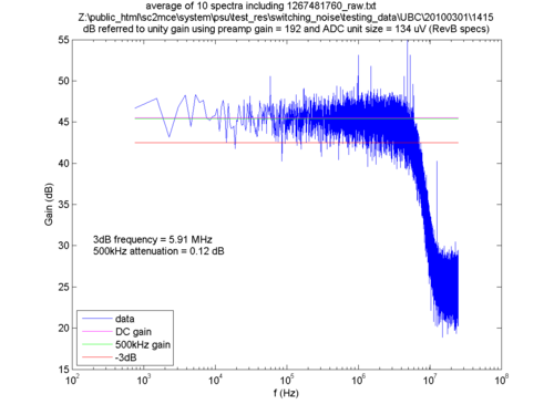
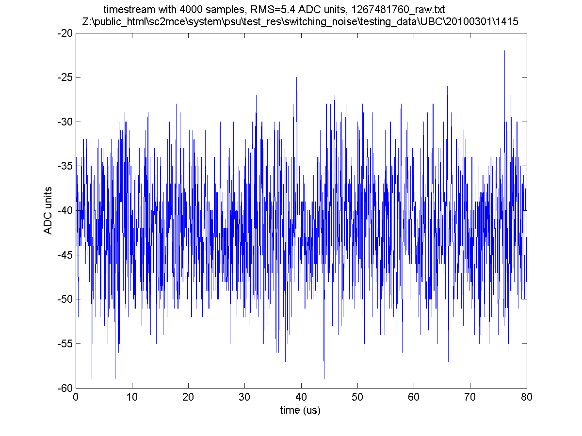
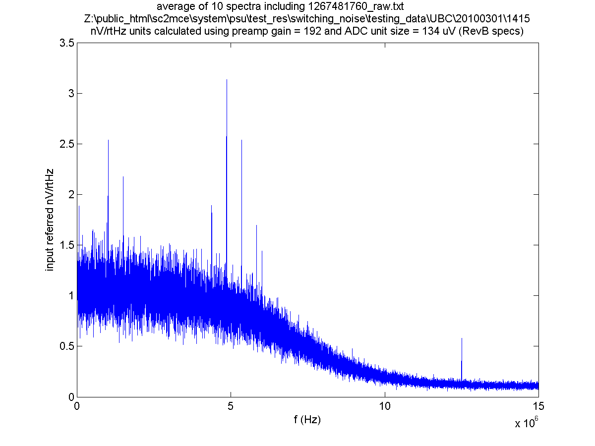
| B9 | 5.4 ADC units | 5.91 MHz | 0.12 dB |
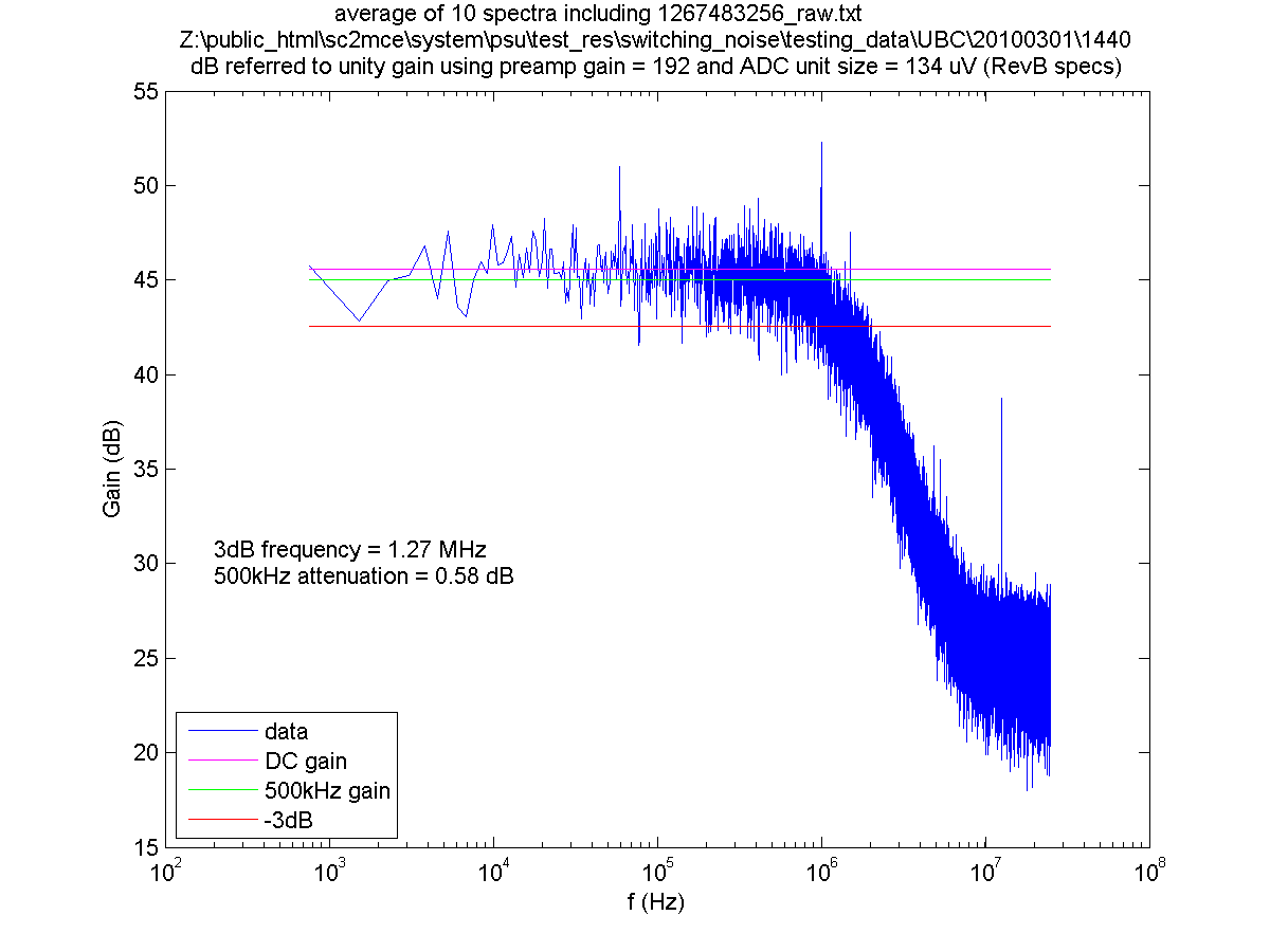
| B10 | 3.0 ADC units | 1.27 MHz | 0.58 dB |
| D0 | 7.9 ADC units | 8.31 MHz | 0.48 dB |
Rev B9
RC Rev B9 Schematic (preamp chain on page 7)
The gain distribution of Revision B is: first stage 4, second stage 4, third stage 6, fourth stage 2, for a total gain of 192. The card uses a 16 bit ADC with a 2.2 V reference, leading to a LSB size of 134 uV. The 3dB cutoff frequency of the chain is about 6 MHz. The noise of the preamp chain is approximately 5.4 ADC units.
Test results using a Revision B9 card are shown below.
Rev B10
The schematic for Rev B10 is identical to that of B9, excepting 3 capacitor value changes on each channel of the preamp. These capacitors were altered to reduce the cutoff frequency of the preamp chain in order to reduce out of band noise. The designed cutoff frequency was reduced from 6MHz to about 1.4 MHz, which predicts a reduction in total noise across the full band of the ADC of approximately Sqrt(1.4/6), or a little bit better than 50%.
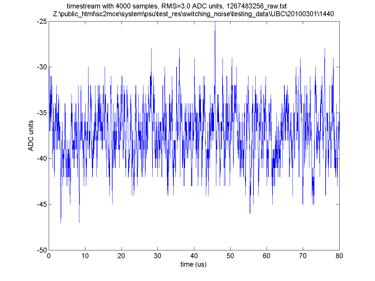
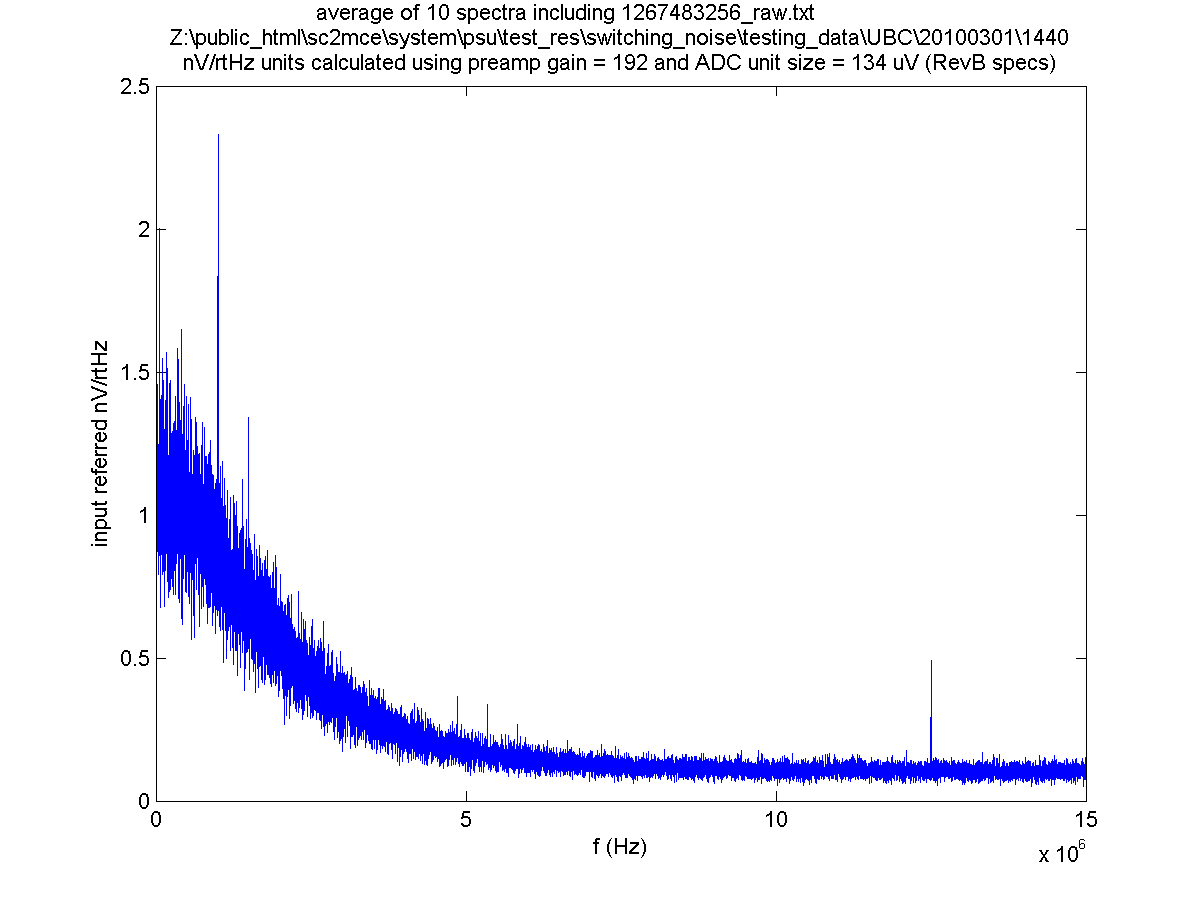
The gain distribution of Revision B is: first stage 4, second stage 4, third stage 6, fourth stage 2, for a total gain of 192. The card uses a 16 bit ADC with a 2.2 V reference, leading to a LSB size of 134 uV. The measured noise was about 3.0 ADC units. The maximum signal frequency of interest (500 kHz) is attenuated by about 0.6 dB by the filter compared to DC gain.
In order to achieve the lower cutoff frequency, capacitors C74, C75 and C76 were altered to 470pF, 470pF, and 68pF respectively. This shifts the pole locations:
pole 1 (R10 & C74) - 3.4 MHz (previously 15.9 MHz in B9)
pole 2 (R20 & C78) - 10.2 MHz (unchanged)
pole 3 (R14 & C75) - 3.4 MHz (previously 15.9 MHz in B9)
pole 4 (R21 & C79) - 10.2 MHz (unchanged)
pole 5 (R16 & C76) - 2.3 MHz (previously 7.2 MHz in B9)
pole 6 (R10&C73, and R24&C77) - 7.2 MHz (unchanged)
The combination of these poles results in a total cutoff frequency (calculated via SPICE simulation using ideal opamps) of 1.44 MHz. The actual cutoff frequency is expected to be slightly lower than this due to the use of AD797 op amps in the first two stages, which have low roll off frequencies (estimated at between 10 and 20 MHz at a gain of 4) that contribute to further reduction of the overall cutoff frequency. The uncertainty in the resistors (1%) and capacitors (5%) result in a maximum variation of overall cutoff frequency between (calculated using SPICE simulation) 1.37 MHz and 1.53 MHz around the nominal value of 1.44 MHz.
Test results using a Revision B10 card are shown below.
Rev D0
RC Rev D Schematic (preamp chain on page 11)
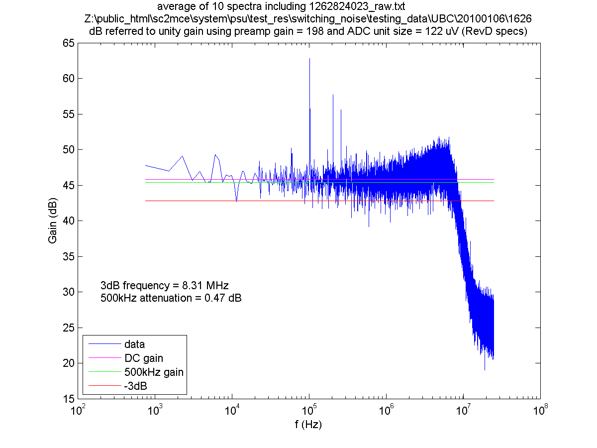
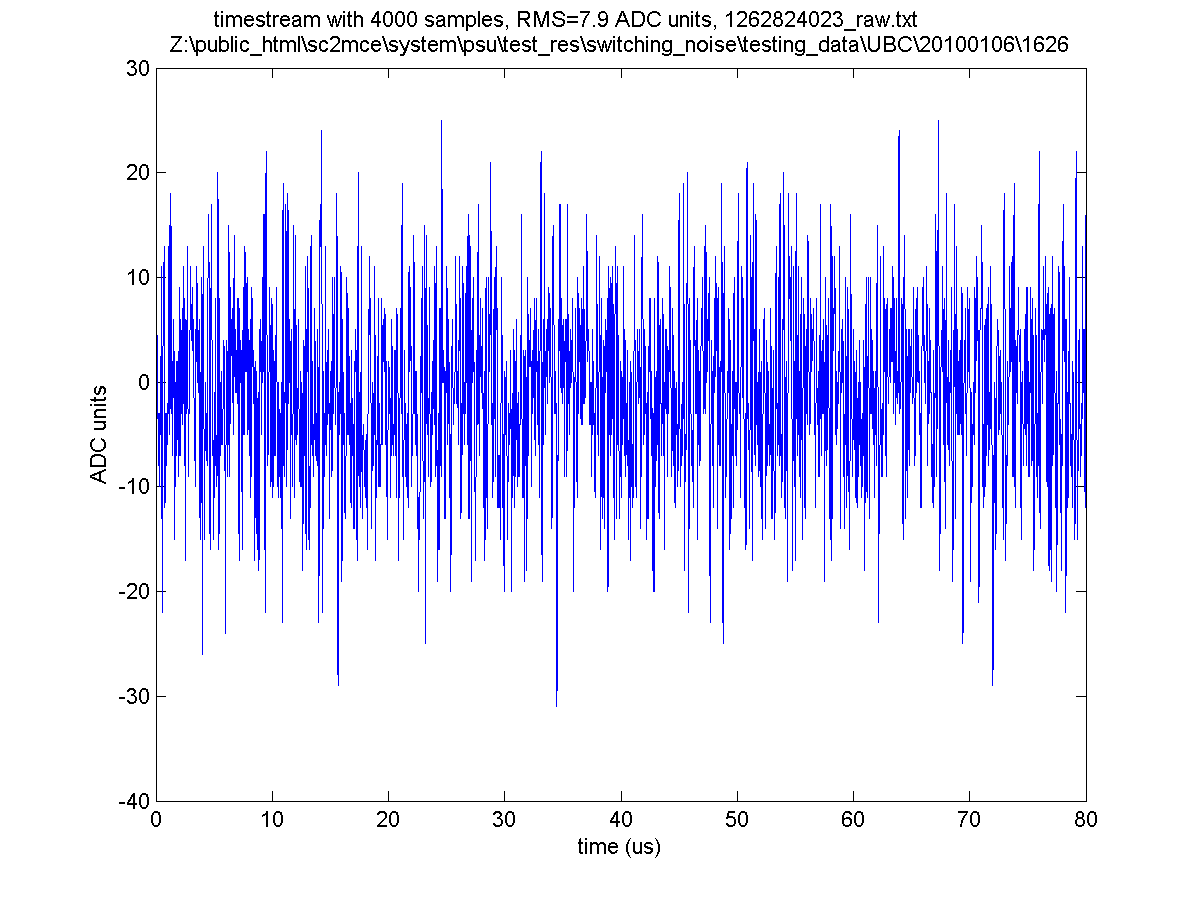
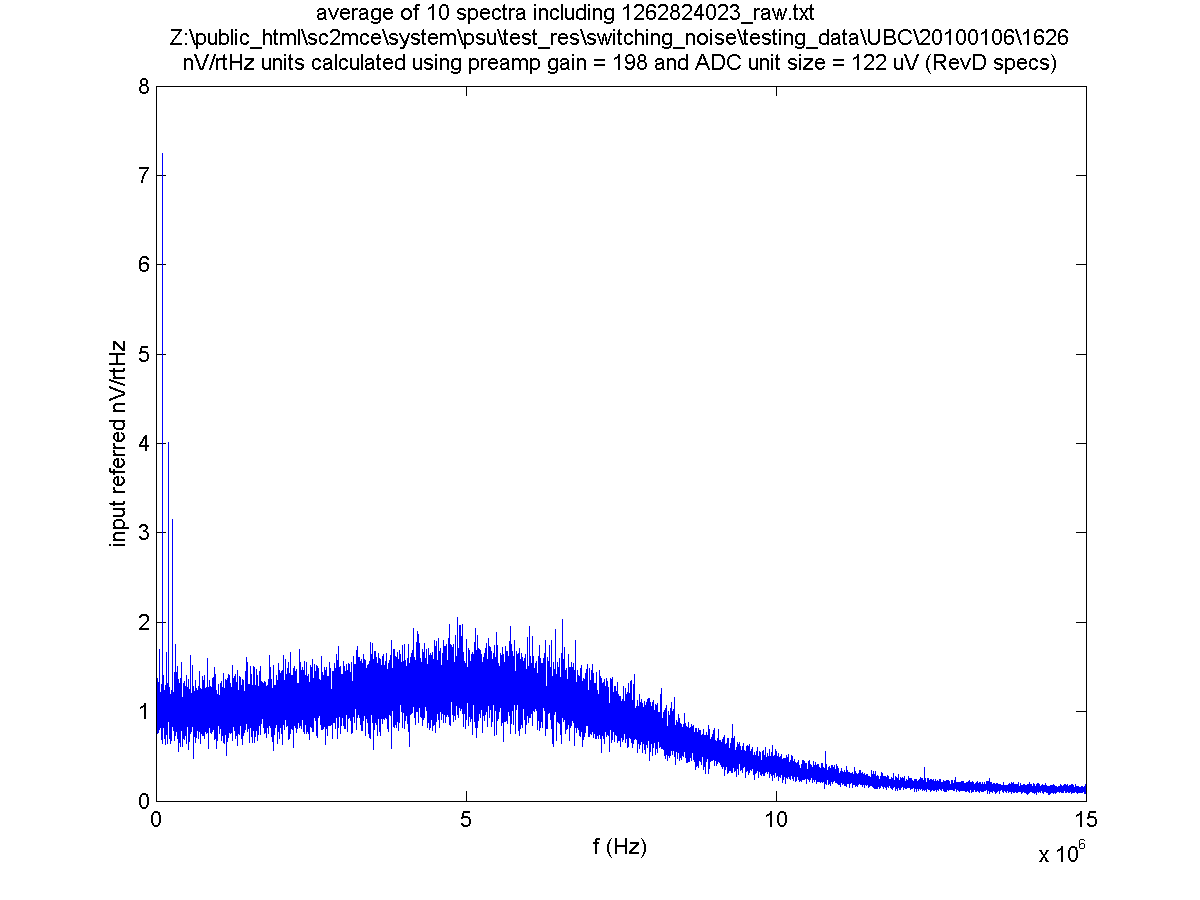
The gain distribution of Revision B is: first stage 5.52, second stage 6, third stage 6, fourth stage 1, for a total gain of 199. The card uses a 16 bit ADC with a 2.0 V reference, leading to a LSB size of 122 uV. Due to the slightly higher early stage gains, an internal opamp resonance of the AD797 used in the first two stages appears in the gain curve shape, resulting in the rise above DC gain in the MHz range before roll off. The filter cutoff frequency is designed to be about 6.7 MHz, but measures approximately 8 MHz. This discrepancy is attributed to the opamp frequency response at relatively low gain and low input signal amplitude. The measured noise was about 7.9 ADC units, although this appears to include some significant external noise in the kHz range.
Test results using a Revision D card are shown below.
